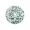
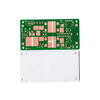
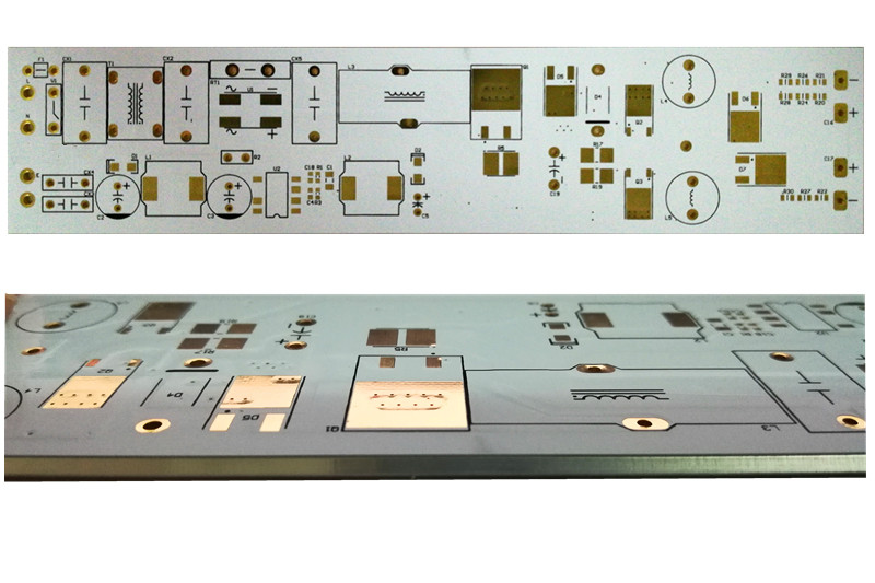
About our product
Heat
is the biggest threat to LEDS and other silicon semiconductors. With
the rapid development of electronic industry, the size of electronic
products is getting smaller and smaller, and the power density is
getting larger and larger. Solving the problem of heat dissipation is a
huge challenge to industrial design. Aluminum Substrate is undoubtedly
one of the effective means to solve the problem of heat dissipation.
Compared
with the traditional FR-4, the aluminum substrate can minimize the
thermal resistance and make the substrate excellent. Compared with the
thick film ceramic circuit, its mechanical properties are excellent.
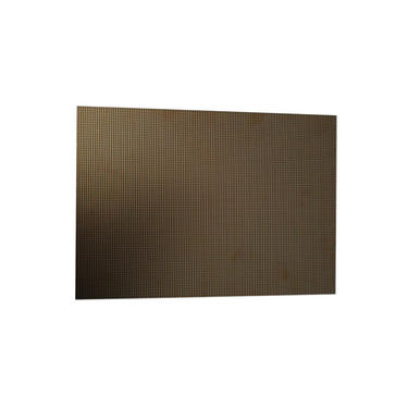
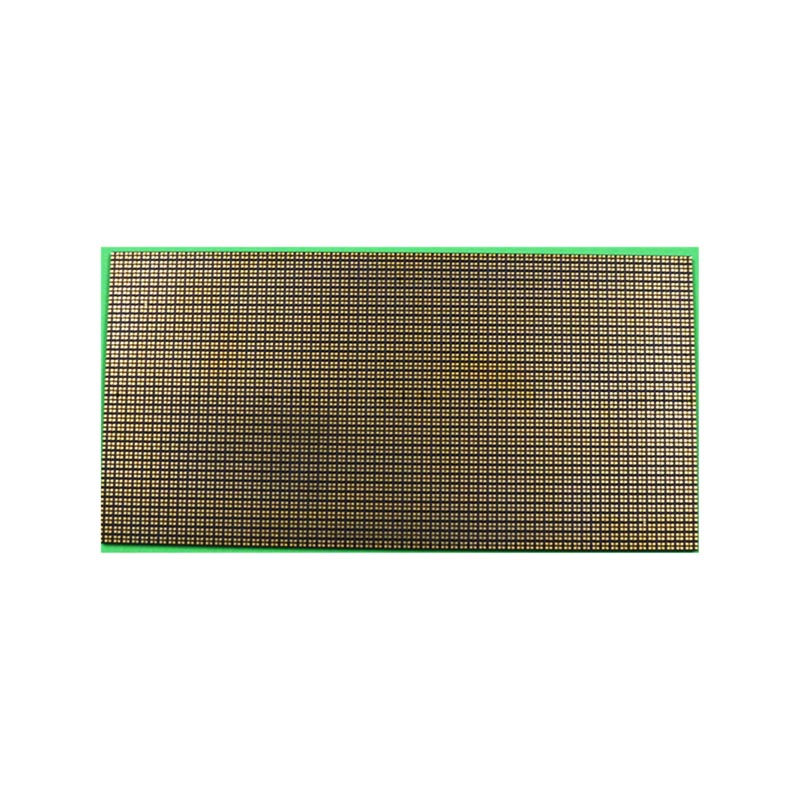
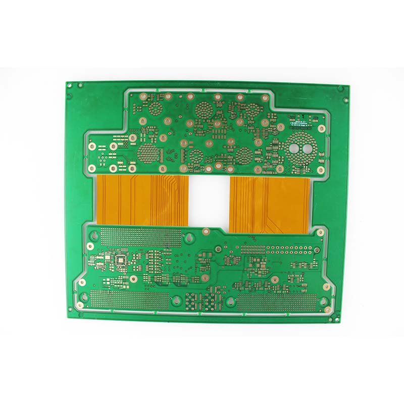
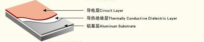
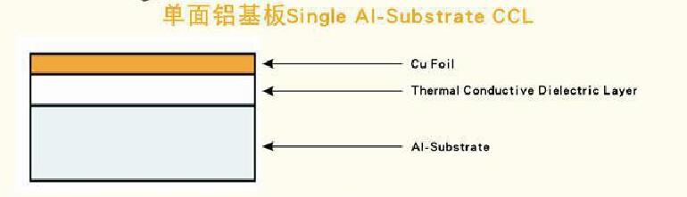
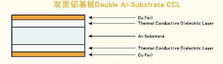
Aluminum
substrate is a kind of copper clad laminate with good heat dissipation
function. It consists of a unique three-layer structure, namely, circuit
layer, thermal conductive insulation layer and metal base layer.
There are also the following unique advantages,
Compliance with RoHs requirements
In the design of electric circuit, thermal diffusion can be treated effectively.
Reducing the operating temperature of the module, prolonging the service life, increasing the power density and reliability
Reduce
the assembly of radiator and other hardware (including thermal
interface materials), reduce module size, and reduce hardware and
assembly costs;
Replacing fragile ceramic substrates for better mechanical durability
VS
> Our factories have invested heavily in importing advanced production facilities from abroad. Such as Burkle laminator, Mitsubishi laser drill, Hitachi mechanical drill, Japan screen automatic exposure machine, LDI, AOI etc, highly automated manufacturing. With a monthly output of up to 250,000 square meters.
> Our suppliers have formed a complete production process, become more professional, modern and large-scale, and signed long-term strategic cooperation agreements with well-known enterprises at home and abroad.
> Under the system of ISO 9001, ISO 14001, ISO/TS16949, OHSAS 18001, ISO/IEC27001, UL, SGS and RoHS, we have guaranteed our excellent quality and leading market position with strong technical development momentum. We also adhere to the 5S method, lean and Six Sigma quality system.
> We provide real-time and in-depth technical support. We offer the most effective and flexible solution for you. Such as high speed, large capacity, high frequency, mixed pressure (hybrid structure), heat dissipation metal base solutions.
> Free DRC and DFM. Elite engineers with years of experience provide you with free and comprehensive engineering review and support.
> Rapid feedback on the layout, build-up, panels, impedance, material selection, design rules, manufacturability, costs of different solutions, use of micro vias, gold plating, special laminates and other engineering questions. When providing innovative solutions for our customers'products, we always consider maximizing the benefits for our customers.
> Rocket provides industry-leading support to our customers,we are more willing to help customers grow.
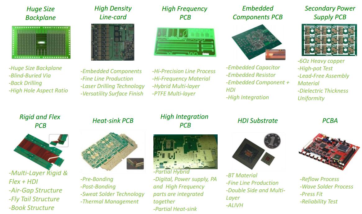
Advanced Product and Advanced Technology
> Quotation for standard projects within 2 hours, quick 24 hours PCB prototype making.
> Multiple different product lines meet the requests of fast delivery of small batches and multi-variety prototyping and mass production.
> Expedited production line for prototyping double-sided PCB up to 24 hours, 4 layers 48 hours, 6 layers 72 hours etc.
> Mass production of double-sided PCB 5-6 days lead time, multi-layer PCB 7-9 days for standard boards.
> DHL, FedEx, TNT, UPS Express, fully meet the customer's rapid turnover requirements, punctual delivery rate of more than 99%.
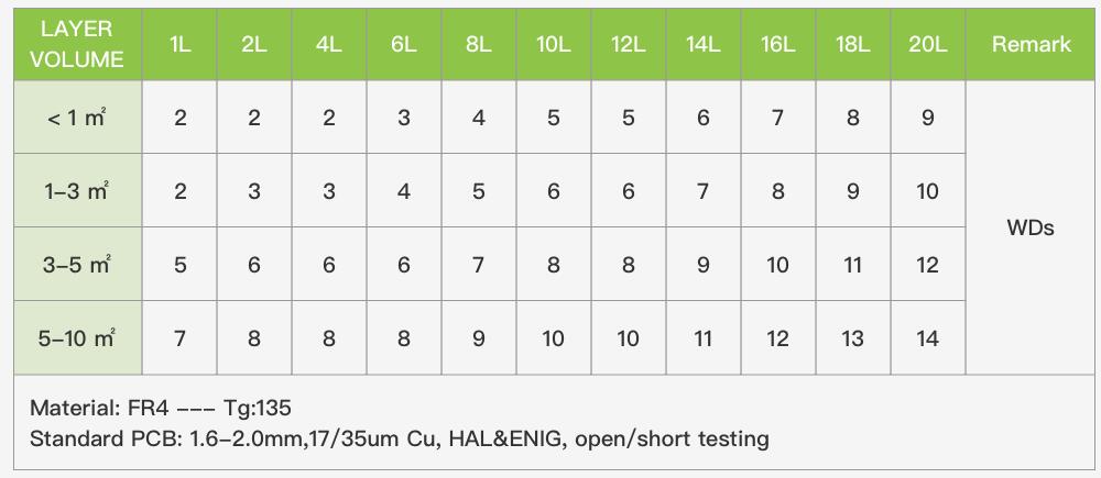
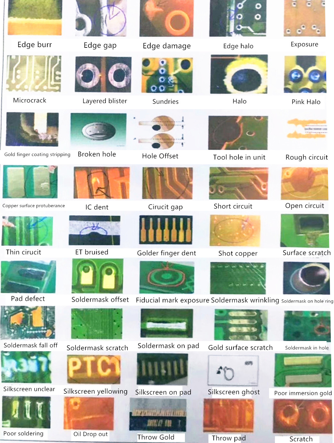
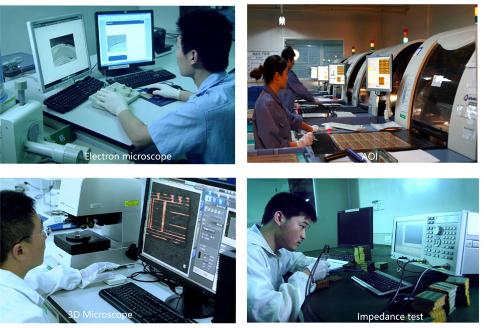
> Dozens of tests such as open/short
circuit testing( ET test), AOI, X-ray, impedance testing, solderability
testing, thermal shock testing, metallographic micro-slicing analysis,
halogen-free testing, etc. 100% outgoing pass rate.
>
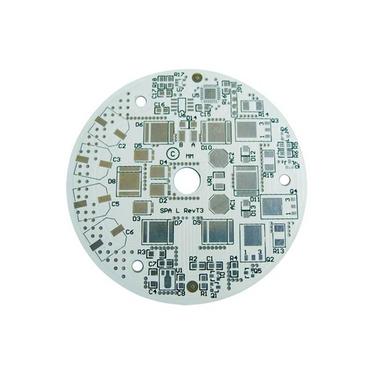
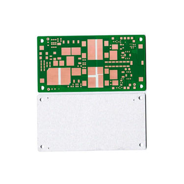
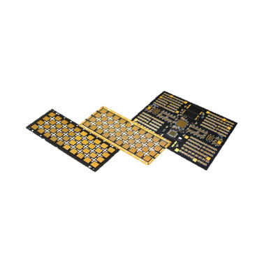
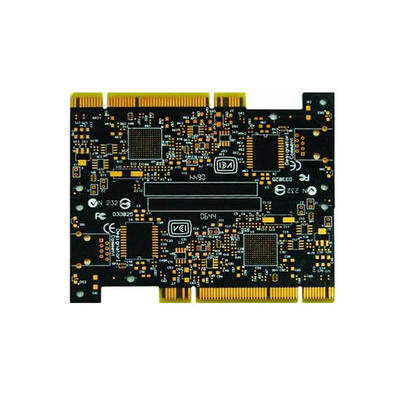
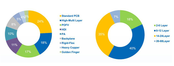
Provide 1-64 layers of different thickness, different materials,
different processes of product customization, of which the CCL using
A-class raw materials, high quality assurance.
> Unlimited
PCB capabilities,we provide various and advanced technology PCBs
include rigid, FPC,
rigid-flex, metal core, microwave/RF, HDI, any layer, heavy copper,
large-size, embedded, LED, backplane, ceramic substrate, IC substrate,
high-frequency,
high-density and high-performance PCB.
> Eight major surface treatment technology and high-quality ink printing, beautiful and reliable.
In Rocket, with advanced production equipment, excellent PCB solutions
and complete testing methods, we have specialists working on their
particular fields with the thorough mastery of their particular
discipline in each of the production facilities. Training, as well as
technical exchanges, are held frequently, tackling problems in key
technologies and configuring scheme of equipment and allowing
professionals to get up to speed on the essential tools that many
organizations value today in the manufacturing industry. Thanks to those
above, we have greatly improved the strength and won international
reputation.
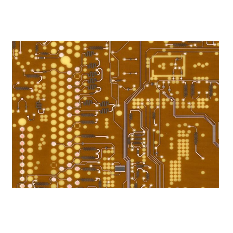
SPECIALIZED MANUFACTURING
Conductive materials and core-to-core bonding
Embedded components
RF connector attachment
Laser direct imaging (LDI)
Laser etching
Laser forming
Multi-level cavity construction
Plated cavities and edges
Composite/hybrid Structures
N+N dual press-fit
Dual-drill
Bonding on metal core
Bulid-up HDI
Long-short and staged gold finger
A wide range of professional manufacturing solutions, can be used for thermal energy (CTE) structural coefficients, thermal challenge design and application, extreme and unique HDI structures, and RF control
A wide range of professional manufacturing solutions, can be used for thermal energy (CTE) structural coefficients, thermal challenge design and application, extreme and unique HDI structures, and RF control
A wide range of professional manufacturing solutions, can be used for thermal energy (CTE) structural coefficients, thermal challenge design and application, extreme and unique HDI structures, and RF contro
CAPABILITIES
3mil line and space
4mil laser defined vias
6mil chip-on-board
6mil mechanically drilled vias
Conductive and non-conductive via fill
Dual backdrilling
Sequential lamination
Mixed dielectric
Heatsink Bonding
Heavy copper/thermal vias
Blind/buried vias
Stacked and staggerd microvias
EXTENSIVE ANALYTICAL TESTING![]()
Design Rules Check(DRC)
Electrical Testing
Automated Optical Inspection(AOI)
X-Ray
Plating thickness testing
Metalized vias inspection
Thermal shock testing
Surface peelability testing
Impedance control testing
100% visual inspection
Solderability testing
Ionic cleanliness testing
Metallographic microscopic analysis
High voltage testing
Insulating resistance testing
FEATURES
PTFE
High speed/low loss
High temperature
Low CTE
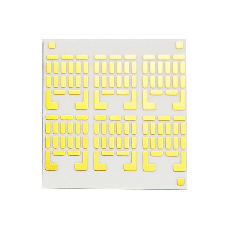
Lead-free, HASL, ENIG, EPENIG, Immersion Silver, Tin, Gold finger
Combination surface finished
Copper-filled microvias
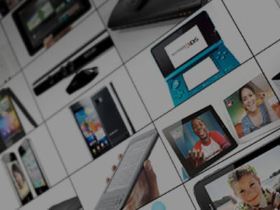
Consumer electronics
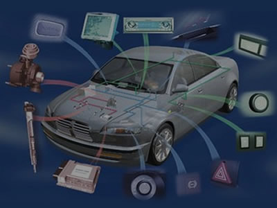
Automotive electronics

Communications
Energy
Industrial & Instrumentation

IOT/Smart Home

Medical electronics

Security Industry