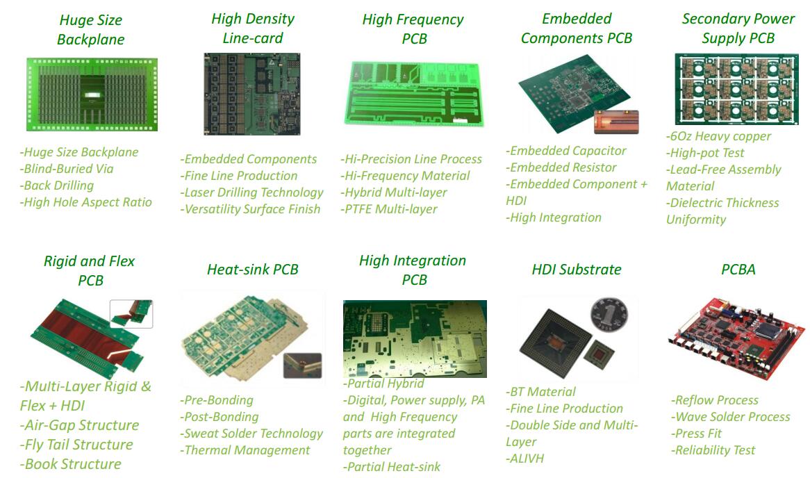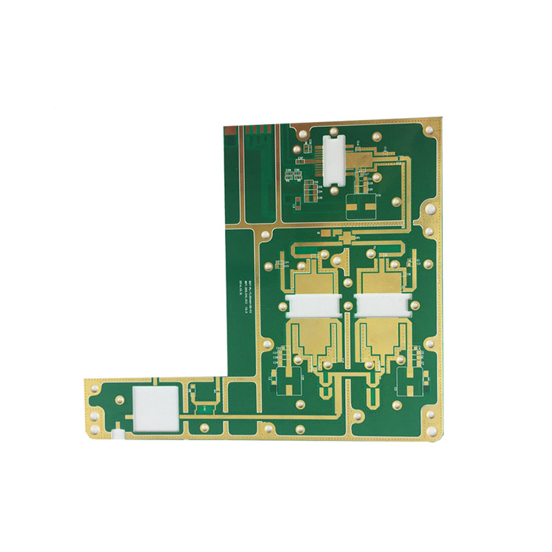

SPECIALIZED MANUFACTURING
Conductive materials and core-to-core bonding
Embedded components
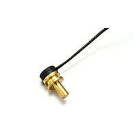
RF connector attachment
Laser direct imaging (LDI)
Laser etching
Laser forming
Multi-level cavity construction
Plated cavities and edges
Composite/hybrid Structures
N+N dual press-fit
Dual-drill
Bonding on metal core
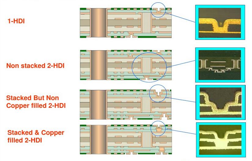
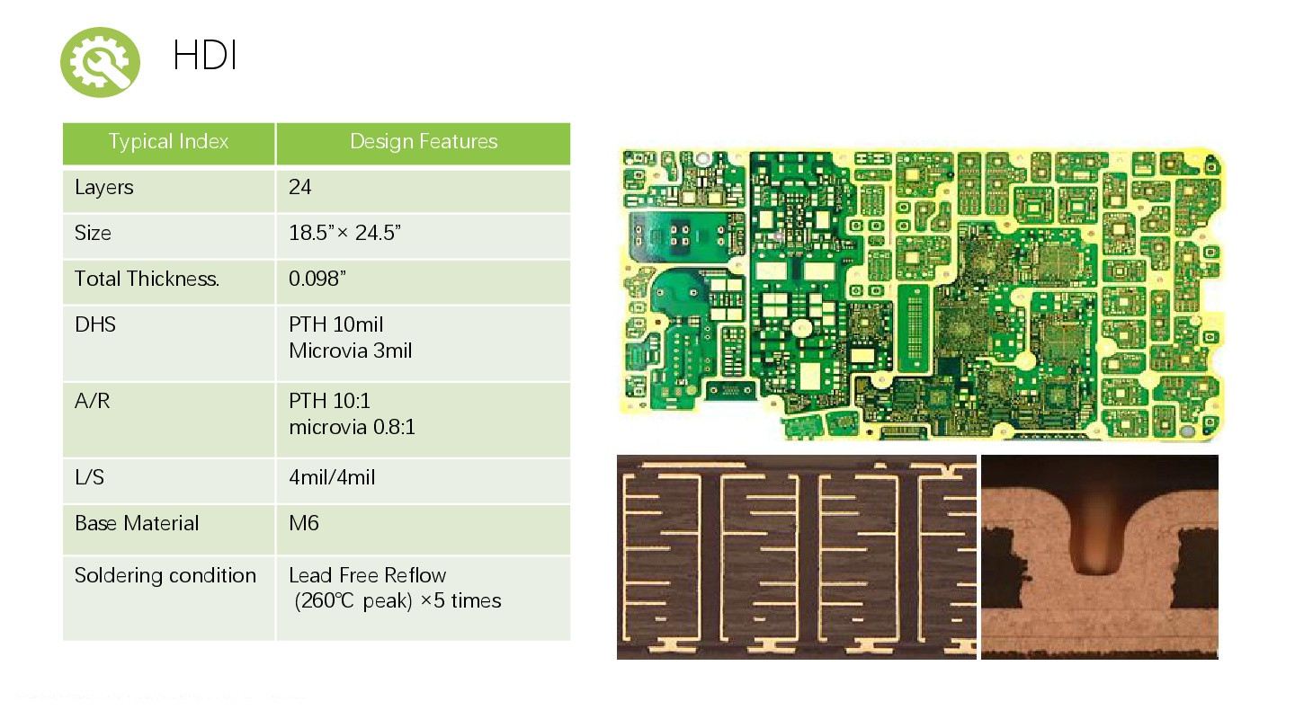
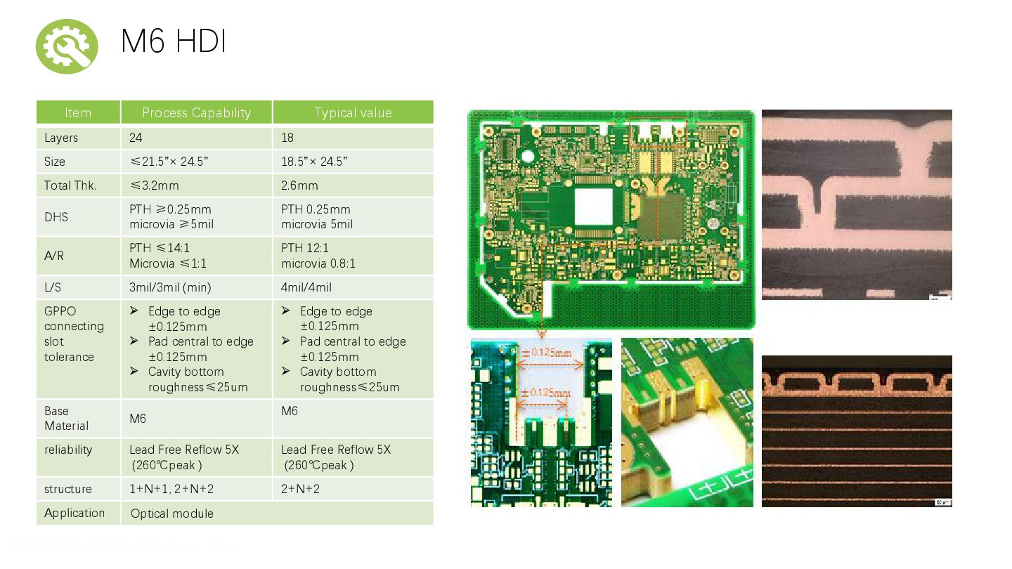
Bulid-up HDI
Long-short and staged gold finger
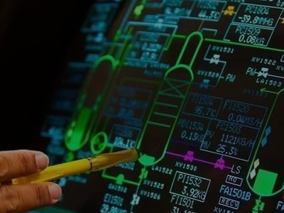
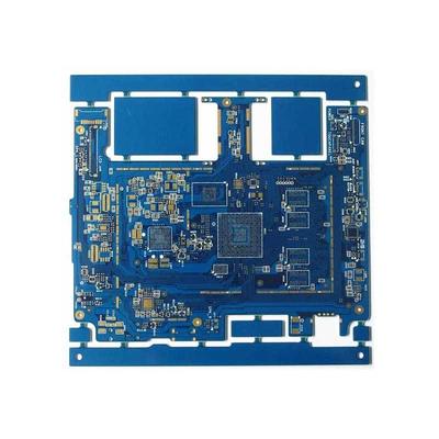
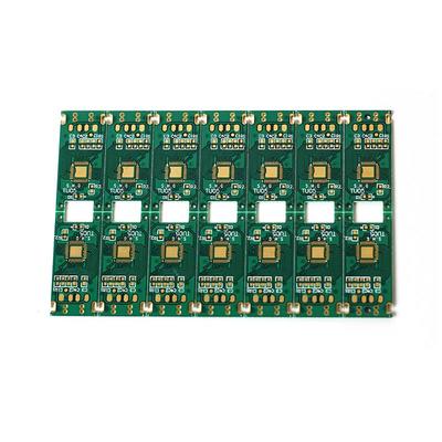
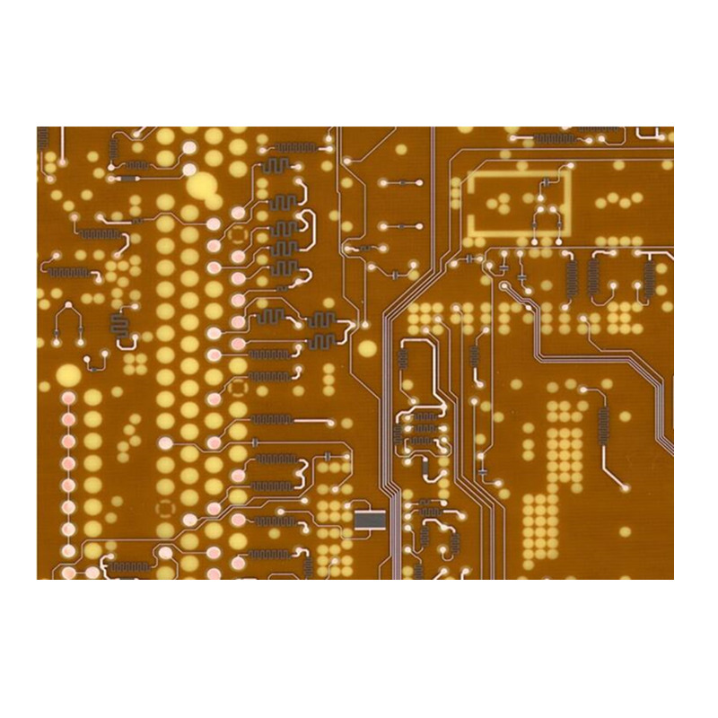
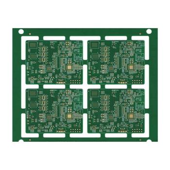
A wide range of professional manufacturing solutions, can be used for thermal energy (CTE) structural coefficients, thermal challenge design and application, extreme and unique HDI structures, and RF control
A wide range of professional manufacturing solutions, can be used for thermal energy (CTE) structural coefficients, thermal challenge design and application, extreme and unique HDI structures, and RF control
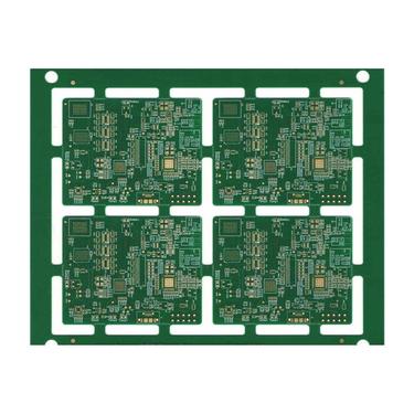
A wide range of professional manufacturing solutions, can be used for thermal energy (CTE) structural coefficients, thermal challenge design and application, extreme and unique HDI structures, and RF contro