01
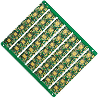
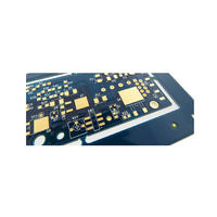
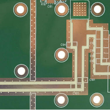
Rogers 4350B Mixed Pressure FR4 PCB

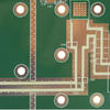
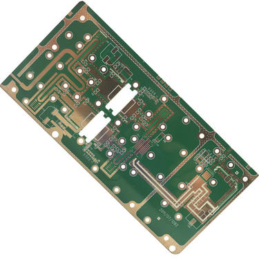
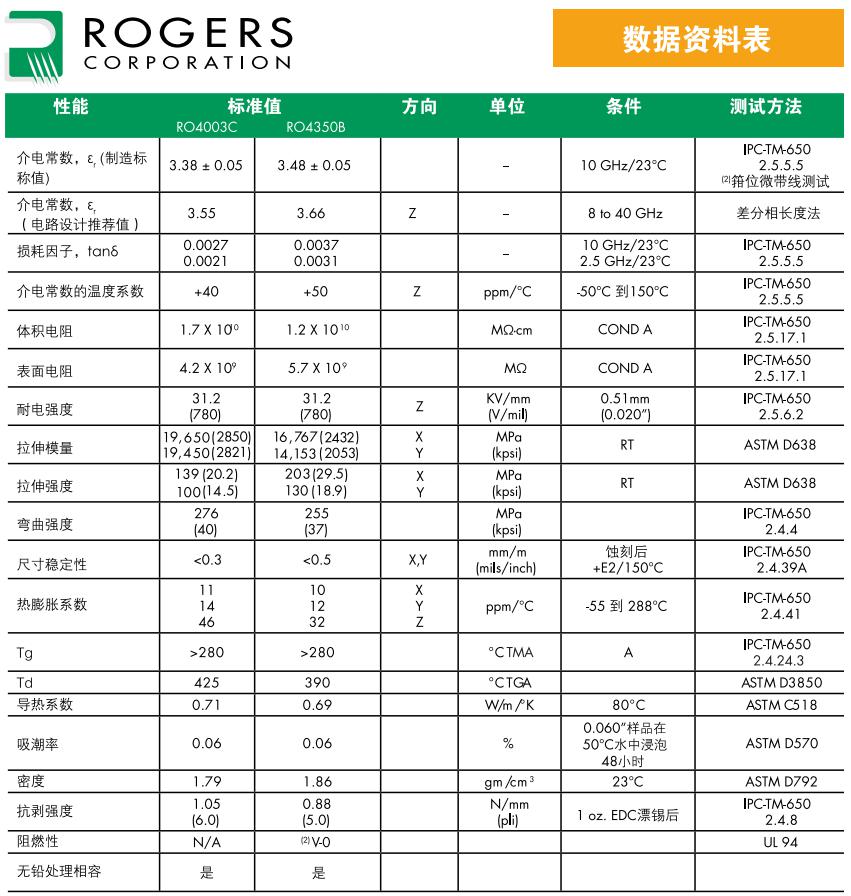
Rogers 4003C with FR4 hybrid stackup PCB; Rogers 4350B mixed FR4 PCB; Rogers 5880 stack up FR4; Signal layer use Rogers material, and the second layer use FR4; Rogers and FR4 mix design is much more cheaper than Rogers+rogers.

| Item | Manufacturing Capabilities | Remark | ||||||
| Material | ||||||||
| Material | Shengyi FR-4 | Normal TG, Medium TG and High TG | ||||||
| HF | Medium TG and High TG | |||||||
| Ceramic filled High Frequency Board | Rogers 4003/4350, Arlon 25N/25FR | |||||||
| PTFE High Frequency Board | Rogers series, Arlon series, Taconic series | |||||||
| Specification | ||||||||
| Surface Finish | HASL with Lead/HASL LEAD FREE | Tin Thickness | 2-40um | |||||
| Board Thickness | 0.6mm≤H≤3.0mm | |||||||
| Immersion Gold (ENIG) | Max. Gold Thickness | 8u" | ||||||
| OSP | Film Thickness | 0.2-0.5um | ||||||
| Hard Gold | Max. Gold Thickness | 2.0um | ||||||
| Immersion Tin | Tin Thickness | 0.8-1.2um | ||||||
| Immersion Silver | Silver Thickness | 0.15-0.25um | ||||||
| Layers | 4 - 40 layers | FR4 Max. 40 layers | ||||||
| Finished Board Thickness | 0.2-6.8 mm | Min. Thickness: 0.2mm (Double-Sided) | ||||||
| Thickness Tolerance | T≥1.0mm | ±10% (Standard PCB) | ±8% (Advanced PCB) | / | ||||
| T<1.0mm | ±0.1mm (Standard PCB) | ±10% (Advanced PCB) | / | |||||
| Finished Copper Thickness | 1oz/2oz (Standard PCB) | Inner Layer: 12oz (Advanced PCB) | 1oz = 35um | |||||
| Outer Layer: 15oz (Advanced PCB) | ||||||||
| Bow and Twist | Per Cater-Corner Length, ≤0.75% (Standard PCB) | ≤0.50% (Advanced PCB) | For Boards without SMT, the max. 1.5% | |||||
| Drill | ||||||||
| PTH Deviation | ±3mil (Standard PCB) | ±2mil (Advanced PCB) | ||||||
| NPTH Deviation | ±2mil (Standard PCB) | ±1mil (Advanced PCB) | ||||||
| Hole Position Deviation | ±3mil (Standard PCB) | / | ||||||
| Hole Wall Roughness (Max.) | 1.5mil (Standard PCB) | 1mil (Advanced PCB) | ||||||
| Min. Drilling Bit Diameter | 0.3mm (Standard PCB) | 0.25mm (Advanced PCB) | ||||||
| Max. Drilling Bit Diameter | 6.5mm (Standard PCB) | / | For vias larger than 6.5mm, multiple drilling or milling is recommended | |||||
| Min. Slot Width | 0.6mm (Standard PCB) | / | For HASL, the min. finished slot width is 0.45mm, for other surface finish, it is 0.5mm | |||||
| Board Thickness/Via Diameter | ≤6:1 (Standard PCB) | ≤7:1 (Advanced PCB) | 7:1≤value≥6:1, add one more day for fabrication | |||||
| PTH Deviation | Width | ±4mil (Standard PCB) | / | |||||
| Length | ±5mil (Standard PCB) | / | ||||||
| NPTH Deviation | Width | ±3mil (Standard PCB) | / | |||||
| Length | ±4mil (Standard PCB) | / | ||||||
| Hole Wall Copper Thickness | Thinnest | ≥0.71mil (Standard PCB) | ≥1mil (Advanced PCB) | |||||
| Average | ≥0.8mil (Standard PCB) | ≥1mil (Advanced PCB) | ||||||
| VIA Space (Same Net) | ≥8mil (Standard PCB) | ≥6mil (Advanced PCB) | ||||||
| VIA Space (Different Net) | ≥17mil (Standard PCB) | ≥14mil (Advanced PCB) | ||||||
| Min. Space for Component VIAs in Different Net | ≥24mil (Standard PCB) | ≥20mil (Advanced PCB) | ||||||
| Max. PTH | Round Hole | 8mm (Standard PCB) | 10mm (Advanced PCB) | |||||
| Slot Holes | 6*10mm (Standard PCB) | 8*12mm (Advanced PCB) | ||||||
| Trace | ||||||||
| Min. Trace Width/Space | 1oz | 6/6mil (Standard PCB) | 5/5mil (Advanced PCB) | The space refers to the distance between trace to trace, trace to copper | ||||
| 2oz | 8/8mil (Standard PCB) | 7/7mil (Advanced PCB) | ||||||
| Min. SMD Width | 1oz | ≥10mil (Standard PCB) | ≥8mil (Advanced PCB) | / | ||||
| 2oz | ≥12mil (Standard PCB) | ≥10mil (Advanced PCB) | ||||||
| Space between Pad to Trace | 1oz | 8mil (Standard PCB) | 6mil (Advanced PCB) | / | ||||
| 2oz | 8mil (Standard PCB) | 6mil (Advanced PCB) | ||||||
| Min. Etching Letters | ≥8mil (Standard PCB) | ≥7mil (Advanced PCB) | ||||||
| Min. Space for SMD | ≥10mil (Standard PCB) | / | The data is the Min. space to achieve Solder Mask Bridge, if Bridge is not required, please refer to the Min. Trace Space requirement | |||||
| V-Cut Line to Copper | T≥1.5mm, V-Cut 20° | 20mil (Standard PCB) | 16mil (Advanced PCB) | |||||
| T≤1.2mm, V-Cut 20° | 16mil (Standard PCB) | 12mil (Advanced PCB) | ||||||
| Trace Width/Space Deviation | ±20% (Standard PCB) | ±15% (Advanced PCB) | ||||||
| Trace Net Grids | 12/12mil (Standard PCB) | 8/8mil (Advanced PCB) | ||||||
| Alignment Accuracy for Layer | ±3mil (Standard PCB) | ±2mil (Advanced PCB) | ||||||
| Space between Trace and Border | Inner layer | ≥16mil (Standard PCB) | ≥12mil (Advanced PCB) | If there is V-Cut requirement, please follow the V-Cut standards | ||||
| Outer layer | ≥10mil (Standard PCB) | ≥8mil (Advanced PCB) | ||||||
| Space between Via to Trace | ≥12mil (Standard PCB) | ≥10mil (Advanced PCB) | ||||||
| Space between Inner Via to Trace | ≥10mil (Standard PCB) | ≥8mil (Advanced PCB) | ||||||
| Solder Mask | ||||||||
| Solder Oil Thickness | Trace Interface | 0.4-0.8mil (Standard PCB) | / | |||||
| Trace Corner | ≥0.2mil (Standard PCB) | / | ||||||
| Plugged Via Diameter | Plugged on both sides | ≤0.45mm (Standard PCB) | 0.5-0.55mm (Advanced PCB) | No solder mask opening on both sides | ||||
| Plumpness for Plugged Vias(Max.) | 100%(Vias Diameter≤0.4mm) (Standard PCB) | 50%(Vias Diameter≤0.45mm) (Advanced PCB) | Refer to plugged depth | |||||
| Space between Opening to Trace/Copper | ≥4mil (Standard PCB) | ≥3mil (Advanced PCB) | ||||||
| Opening Size (Single Side) | ≥3mil (Standard PCB) | ≥2mil (Advanced PCB) | ||||||
| Text Width for Solder Mask Opening | ≥10mil (Standard PCB) | ≥8mil (Advanced PCB) | ||||||
| Solder Mask Bridge Width | Green, Blue≥4mil; White, Black≥6mil; others≥5mil | |||||||
| Silkscreen | ||||||||
| Silkscreen Width | Positive Text | ≥6mil (Standard PCB) | 5mil (Advanced PCB) | |||||
| Negative Text | ≥8mil (Standard PCB) | ≥6mil (Advanced PCB) | ||||||
| Silkscreen Height | ≥40mil (Standard PCB) | ≥30mil (Advanced PCB) | ||||||
| Space between Silkscreen to Copper Pad | ≥7mil (Standard PCB) | 6mil (Advanced PCB) | ||||||
| The Distance between Solder Mask Oil to Copper Pad | ≥10mil (Standard PCB) | 8mil (Advanced PCB) | The Min. Solder Mask Oil Strip is 5mil | |||||
| Space between Silkscreen to Border | ≥8mil (Standard PCB) | 6mil (Advanced PCB) | ||||||
| Min. Silkscreen Space | ≥6mil (Standard PCB) | 5mil (Advanced PCB) | ||||||
| V-CUT | ||||||||
| Min. Dimension | 80*80mm (Standard PCB) | / | Only for V-Cut with one direction, the min. size is 40mm for the side without V-Cut | |||||
| Max. Dimension | 500*500mm (Standard PCB) | Max. Width for manual V-Cut board is 500mm, not limited for length | ||||||
| Min. Board Thickness | 0.6mm (Standard PCB) | / | No V-cut for 0.4mm board | |||||
| V-CUT Angle | 20°/30° (Standard PCB) | / | ||||||
| Alignment Accuracy for Neighbouring V-CUT | ±0.1mm (Standard PCB) | / | ||||||
| Space for two V-CUT Lines | ≥3mm (Standard PCB) | / | ||||||
| Space between Border to first V-Cut Line | ≥3mm (Standard PCB) | / | ||||||
| Remaining Board Thickness after V-Cut | 1/3 or 1/4 of Board Thickness (Standard PCB) | / | Min. remaining thickness 0.25mm | |||||
| Remaining Board Thickness Deviation after V-Cut | ±0.1mm (Standard PCB) | / | ||||||
| Profiling | |||||||
| CNC Routing Deviation | ±0.15mm (Standard PCB) | ±0.10mm (Advanced PCB) | |||||
| CNC the Distance Deviation between Via to Border | ±0.13mm (Standard PCB) | ±0.10mm (Advanced PCB) | |||||
| Min. Slot Width | 0.8mm (Standard PCB) | / | |||||
| CNC Min. Via Corner Angle for Routing | 0.4mm (Standard PCB) | / | |||||
| Min. PCB Dimension | 5*5mm (Standard PCB) | Min. 3mm for one side (Advanced PCB) | |||||


Contact
Supplier