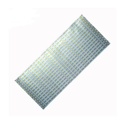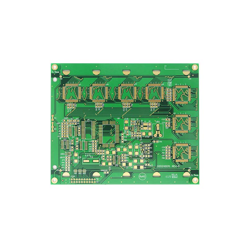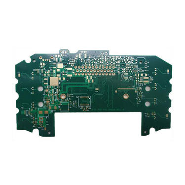
Multilayer PCB 8 layers FR4(TG170) material Immersion Gold Finish
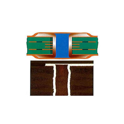
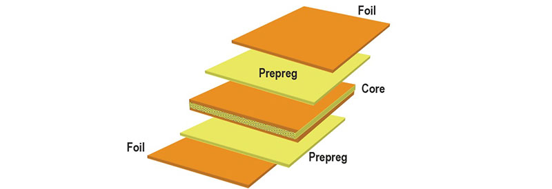
Multilayer PCB has more than two conductive copper layers which mainly consist of inner layer cores, prepreg layers and copper foils and they’re melted together through heat and pressure. Lamination process is one of the key to control good quality of multilayer PCB, this process requires specific heating and pressure for specific periods of time based on materials used to ensure the PCB board is made properly.
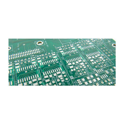
The multilayer PCB is the development of the double sided PCB with increasing complexity and density of components, they allowed the designers to produce highly complex and compact circuits and further development of blind and buried via hole technology has pushed these limits even further. With the requirements of higher precision in various applications, the demands of multilayer PCB keep increasing continuously in recent years. The typical applications of multilayer printed circuit boards include Computers, Data storage, Cell phone transmission, GPS technology, satellite systems and so on.
The benefits of multilayer PCB
● Increased flexibility
● Higher assembly density
● Smaller size(considerable savings on space)
● Easier incorporation controlled impedance features
● Reduces the need for interconnection wiring harnesses(Reduces overall weight)
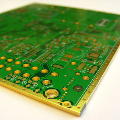
A-TECH is an experienced multilayer PCB manufacturer which own complete multilayer PCB manufacturing process in house from inner layer, vacuum lamination to surface finishes, it brings us more advantages in the competition of global market shares for multilayer printed circuit boards on quality, price and lead time. Currently the proportion of multilayer PCB we manufactured is more than 65%.
| General Specification for multilayer PCB in A-TECH | |
| Layer Count | 4~30 Layers |
| Material Available | FR4, High Tg FR4, PI, Teflon, Rogers. |
| Max board size | 550*650mm |
| Board thickness | 0.4-5.0mm |
| Finished copper thickness | 0.5-6oz |
| Min trace width/spacing | 3/3mil |
| Min hole size | 0.15mm |
| Colour of Solder Mask | Green, Blue, White, Black, Yellow, Red. |
| Colour of Silkscreen | White, Black, Yellow. |
| Surface treatment | HASL, HAL(Lead free), OSP, Gold Plating, Immersion Gold/Tin/Silver, Carbon, Peelable Mask. |
Contact
Supplier