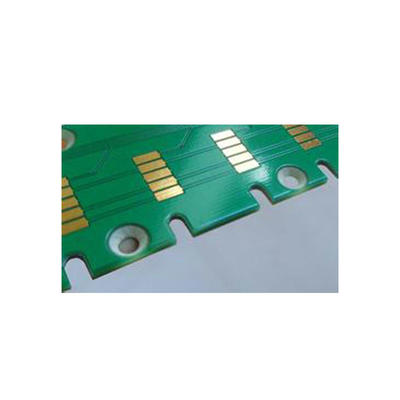


Multilayer Plated Half Hole PCB Half PTH PCB Immersion Gold Finish
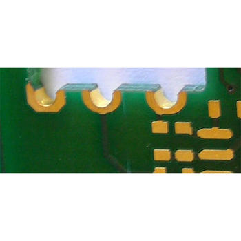
Plated half holes which is also called castellated holes, they’re normally designed at the edge of printed circuit boards and plated with copper, and they’re mainly used for board-on board connections, mostly where two circuit boards with different technologies are combined.
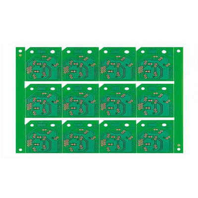
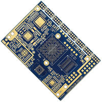
Most of the plated half hole PCBs are a type of modules which are small and high density with fine pitch components, this type of circuit boards are made with GPS Modules, Wifi Modules, Bluetooth Modules, GMS Modules, GPRS Modules and other smart modules.
Basically plated half holes are not suitable for V-score process, because the copper at the hole will be rolled up to cause serious burs, routing process is a better solution to ensure smooth edge.
The guidelines of designing plated half holes
● Normally the minimum half hole size is 0.8mm, it can be min 0.55mm with A-TECH capability
● The routing tolerance for half hole is +/-0.15mm
● The minimum distance from pad to pad is 0.25mm
● Use the larger hole diameter if possible
● Use the larger outer layer pad on both sides if possible
● Connect inner layer pads to the plated holes if possible to bring more stability and help to avoid burrs.
● Routing process is preferred and ENIG finish is preferred.
A-TECH have manufactured a large number of printed circuit boards with half hole design for various module products, and we have obtained rich experience to control high quality, the minimum half hole size we can build is 0.55mm.
Contact
Supplier