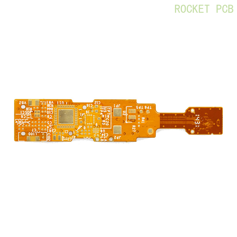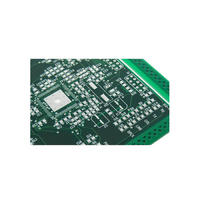

Heavy copper PCB thick copper PCB power supply PCB high quality up to 10 oz
Making process control of thick copper board
Drilling aperture
Due to the need to go through two copper plating, the finished product aperture needs to be compensated accordingly
After two times copper plating need to complete the outer layer pattern, soldermask, silkscreen and other processes, so the Pin hole has the corresponding control
1, Design of first registration pin hole 3.175mm, ensure the accuracy of the first outer layer
2, Design second time of pin holes, due to after two copper plating the pin hole diameter is smaller, so the original design need to do the corresponding compensation, this pin hole directly affect two times of the outer layer, soldermask, silkscreen registration accuracy
First time soldermask control
1, Base material position filling ink, guarantee smooth with copper surface
2, Nail bed making, try to print both sides of soldermask at the same time
3, Block Point Network production, requires 36T mesh yarn
4, Printing ink viscosity ≥300dpa.s, ensure that the substrate and copper surface high difference can fill
5, Pre-baked, after printing static 2H or more
6, Contraposition Wash the remaining ink off the line on the development line, line open window unilateral shrinkage 2-3mil to ensure the accuracy of the position
7, After-baking, segmented baking, to ensure that the substrate position of the ink completely cured
Second time copper Plating
Rough treatment of board surface before drilling and plating, drilling electroplating is the same as double board process , copper plating time 20min , turn off the grinding brush after first time copper plating
Second time outer layer pattern
Pre-treatment turn off the grinding brush, only over pickling, to prevent the substrate bit copper skin wrinkle, to prevent the film from wrinkling resulting in second graphics seepage plating.
> Our factories have invested heavily in importing advanced production facilities from abroad. Such as Burkle laminator, Mitsubishi laser drill, Hitachi mechanical drill, Japan screen automatic exposure machine, LDI, AOI etc, highly automated manufacturing. With a monthly output of up to 250,000 square meters.
> Our suppliers have formed a complete production process, become more professional, modern and large-scale, and signed long-term strategic cooperation agreements with well-known enterprises at home and abroad.
> Under the system of ISO 9001, ISO 14001, ISO/TS16949, OHSAS 18001, ISO/IEC27001, UL, SGS and RoHS, we have guaranteed our excellent quality and leading market position with strong technical development momentum. We also adhere to the 5S method, lean and Six Sigma quality system.
> We provide real-time and in-depth technical support. We offer the most effective and flexible solution for you. Such as high speed, large capacity, high frequency, mixed pressure (hybrid structure), heat dissipation metal base solutions.
> Free DRC and DFM. Elite engineers with years of experience provide you with free and comprehensive engineering review and support.
> Rapid feedback on the layout, build-up, panels, impedance, material selection, design rules, manufacturability, costs of different solutions, use of micro vias, gold plating, special laminates and other engineering questions. When providing innovative solutions for our customers'products, we always consider maximizing the benefits for our customers.
> Rocket provides industry-leading support to our customers,we are more willing to help customers grow with us.
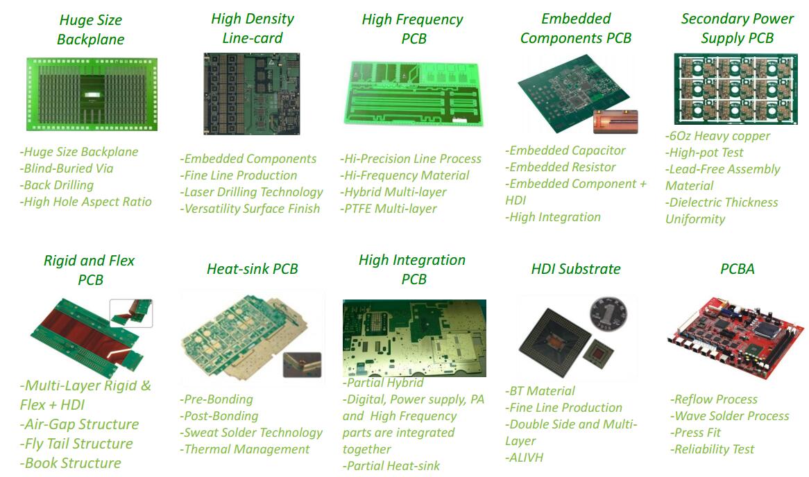
Advanced Product and Advanced Technology
> Quotation for standard projects within 2 hours, quick 24 hours PCB prototype making.
> Multiple different product lines meet the requests of fast delivery of small batches and multi-variety prototyping and mass production.
> Expedited production line for prototyping double-sided PCB up to 24 hours, 4 layers 48 hours, 6 layers 72 hours etc.
> Mass production of double-sided PCB 5-6 days lead time, multi-layer PCB 7-9 days for standard boards.
> DHL, FedEx, TNT, UPS Express, fully meet the customer's rapid turnover requirements, punctual delivery rate of more than 99%.
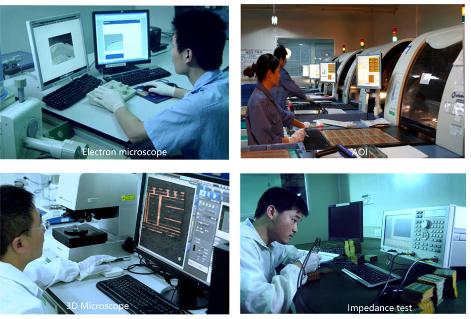
> Dozens of tests such as open/short circuit testing( ET test), AOI, X-ray, impedance testing, solderability testing, thermal shock testing, metallographic micro-slicing analysis, halogen-free testing, etc. 100% outgoing pass rate.
>
Provide 1-64 layers of different thickness, different materials,
different processes of product customization, of which the CCL using
A-class raw materials, high quality assurance.
> Unlimited PCB capabilities,we provide various and advanced technology PCBs include rigid, FPC, rigid-flex, metal core, microwave/RF, HDI, any layer, heavy copper, large-size, embedded, LED, backplane, ceramic substrate, IC substrate, high-frequency, high-density and high-performance PCB.
> Eight major surface treatment technology and high-quality ink printing, beautiful and reliable.


Security Industry
Contact
Supplier