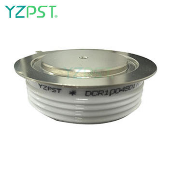
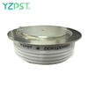

Types of Power Thyristors Phase Control Thyristors 2000V DCR1004
HIGH POWER THYRISTOR PHASE CONTROL
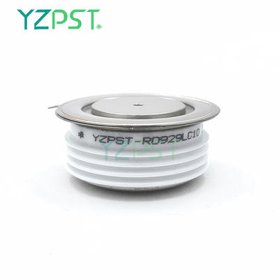
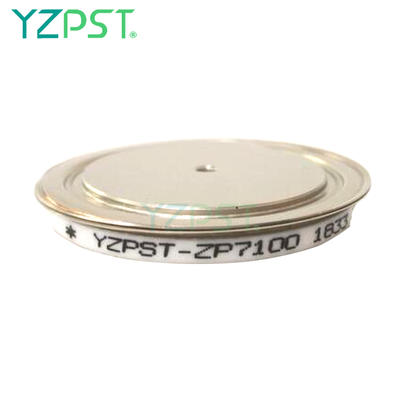
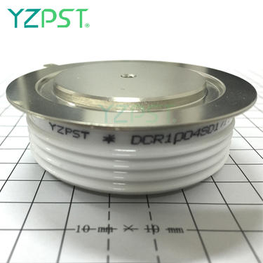
YZPST-DCR1004
DCR1004SD2323
Conducting - on state
Parameter | Symbol | Min. | Max. | Typ. | Units | Conditions |
Average value of on-state current | IT(AV) | 1300 | A | Sinewave,180o conduction,Tc=65oC | ||
RMS value of on-state current | ITRMS | 2000 | A | Nominal value | ||
Peak one cPSTCle surge (non repetitive) current |
ITSM | 20000
18000 | A
A | 8.3 msec (60Hz), sinusoidal wave- shape, 180o conduction, Tj = 125 oC 10.0 msec (50Hz), sinusoidal wave- shape, 180o conduction, Tj = 125 oC | ||
I square t | I2t | 1.7x10⁶ | A2s | 8.3 msec and 10.0 msec | ||
Latching current | IL | 800 | mA | VD = 24 V; RL= 12 ohms | ||
Holding current | IH | 400 | mA | VD = 24 V; I = 2.5 A | ||
Peak on-state voltage | VTM | 1.75 | V | ITM = 3000 A; Duty cPSTCle £ 0.01% | ||
Critical rate of rise of on-state current (5, 6) | di/dt | 600 | A/ms | Switching from VDRM £ 1000 V, non-repetitive | ||
Critical rate of rise of on-state current (6) | di/dt | 200 | A/ms | Switching from VDRM £ 1000 V |
ELECTRICAL CHARACTERISTICS AND RATINGS (cont’d)
Gating
Parameter | Symbol | Min. | Max. | Typ. | Units | Conditions |
Peak gate power dissipation | PGM | 200 | W | tp = 40 us | ||
Average gate power dissipation | PG(AV) | 5 | W | |||
Peak gate current | IGM | 10 | A | |||
Gate current required to trigger all units | IGT | 300 150 125 | mA mA mA | VD = 6 V;RL = 3 ohms;Tj = -40 oC VD = 6 V;RL = 3 ohms;Tj = +25 oC VD = 6 V;RL = 3 ohms;Tj = +125oC | ||
Gate voltage required to trigger all units
| VGT |
0.30 | 5 3
| V V V | VD = 6 V;RL = 3 ohms;Tj = -40 oC VD = 6 V;RL = 3 ohms;Tj = 0-125oC VD = Rated VDRM; RL = 1000 ohms; Tj = + 125 oC | |
Peak negative voltage | VGRM | 5 | V |
Dynamic
Parameter | Symbol | Min. | Max. | Typ. | Units | Conditions |
Delay time | td | 1.5 | 0.7 | ms | ITM = 50 A; VD = Rated VDRM Gate pulse: VG = 20 V; RG = 20 ohms; tr = 0.1 ms; tp = 20 ms | |
Turn-off time (with VR = -50 V) | tq | 250 | 150 | ms | ITM = 1000 A; di/dt = 25 A/ms; VR ³ -50 V; Re-applied dV/dt = 20 V/ms linear to 80% VDRM; VG = 0; Tj = 125 oC; Duty cPSTCle ³ 0.01% | |
Reverse recovery charge | Qrr | * | mC | ITM = 1000 A; di/dt = 25 A/ms; VR ³ -50 V |
* For guaranteed max. value, contact factory.
THERMAL AND MECHANICAL CHARACTERISTICS AND RATINGS
Parameter | Symbol | Min. | Max. | Typ. | Units | Conditions |
Operating temperature | Tj | -40 | +125 | oC | ||
Storage temperature | Tstg | -40 | +150 | oC | ||
Thermal resistance - junction to case | RQ (j-c) | 0.025 0.050 | oC/W | Double sided cooled Single sided cooled | ||
Thermal resistamce - case to sink | RQ (c-s) | 0.010 0.020 | oC/W | Double sided cooled * Single sided cooled * | ||
Mounting force | P | 24.5 | 26.7 | kN | ||
Weight | W | 460 | g |
* Mounting surfaces smooth, flat and greased
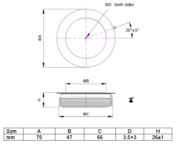
CASE OUTLINE AND DIMENSIONS
Contact
Supplier